NPN transistor
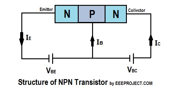
Bipolar junction transistors are of two types mainly. NPN transistor is one of the types of Transistors (BPT). NPN stands for Negative-Positive-Negative configuration. It is the most often used in all type of transistors. Basically, in NPN transistors two n-type (negative) materials dope the single p-type (negative) materials.
In simple words, one p-type semiconductor material is present between the two n-type semiconductor materials. They are the most used type of bipolar junction transistors and the reason behind this is the mobility of their electrons is many times higher than that of the holes (mobility of holes).
Parts of NPN Transistor
This transistor is made of three components or three main regions.
- Emitter
- Base
- Collector
The base is region is very thin and is the region where two diodes are connected back to back. The diode on the left region is referred to as emitter-base diode. And, the diode present in the right side of the circuit is referred to as collector-base diode. The names of both diodes are as per the name of the region they are present in.
The most essential component of this type of transistor is the lightly doped p-region (that is positive). And, the most densely doped region is the collector one. Emitter region is doped moderately when compared to collector and base region.
While making the connections in the circuit, the emitter and base are connected in forward bias, while the collector and base region are connected in reversed bias.
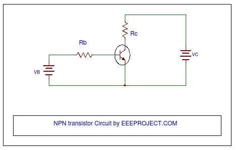
If you want the NPN transistor to work as a type of switch, then the base is connected to the negative supply and the collector is connected to the positive supply. And, then the circuit can be used for switching states that is ‘On’ or ‘Off’.
Working of NPN Transistor
- The emitter-base diode is connected in the forward-bias, whereas the collector-base diode is connected in the reversed-bias.
- In this bipolar junction transistor, the voltage across the emitter-base junction (that is in forward-bias) is always less than the collector-base junction (reversed-bias).
- Most of the charge carriers start moving towards the base; when forward-bias voltage is applied across the emitter.
- And, this movement generates a current in the emitter region which is referred to as ‘emitter current’.
- By passing through the emitter-base junction the carriers enter the base region that is the p-type semiconductor material.
- And, there in the base region these electrons combine with the holes present there.
- As we know that the base region is lightly doped so only few electrons are able to combine with the hole. The rest of the electrons together constitute to form the ‘base current’.
- Then, this current that is the ‘base current’ enters into the collector region via the collector-base junction.
- And, the collector region is connected in the reversed-bias that’s why it applies a high force on the electrons that are coming from the base region through the junction.
- And, thus the collector region collects the electrons.
Applications of NPN Transistor
- Amplifying circuit applications usually have NPN transistors in them.
- They are also used in high frequency applications.
- The NPN Transistor are also present in some classic amplifiers and even in some of the ‘push-pull’ amplifiers.
- They are also used in the temperature sensing devices.
- These transistors are also used as a switch.
- Most of the logarithm converters consist of NPN transistors.
Also watch fm transmitter working explanation

4 thoughts on “NPN Transistor Working and Application [Explained]”
is this transistor used for sound amplifier ?
Please explain MOSFET
I need to use the transistor as a switch. Which transistor should i go for if i have 9 V and 6 A of current ?
Hallo sir!
I have a question that , how the electron will move through Base-collector junction to collector in PNP transistor, while the depletion region between base-collector junction is becoming wider with passage of time because of reverse bias?